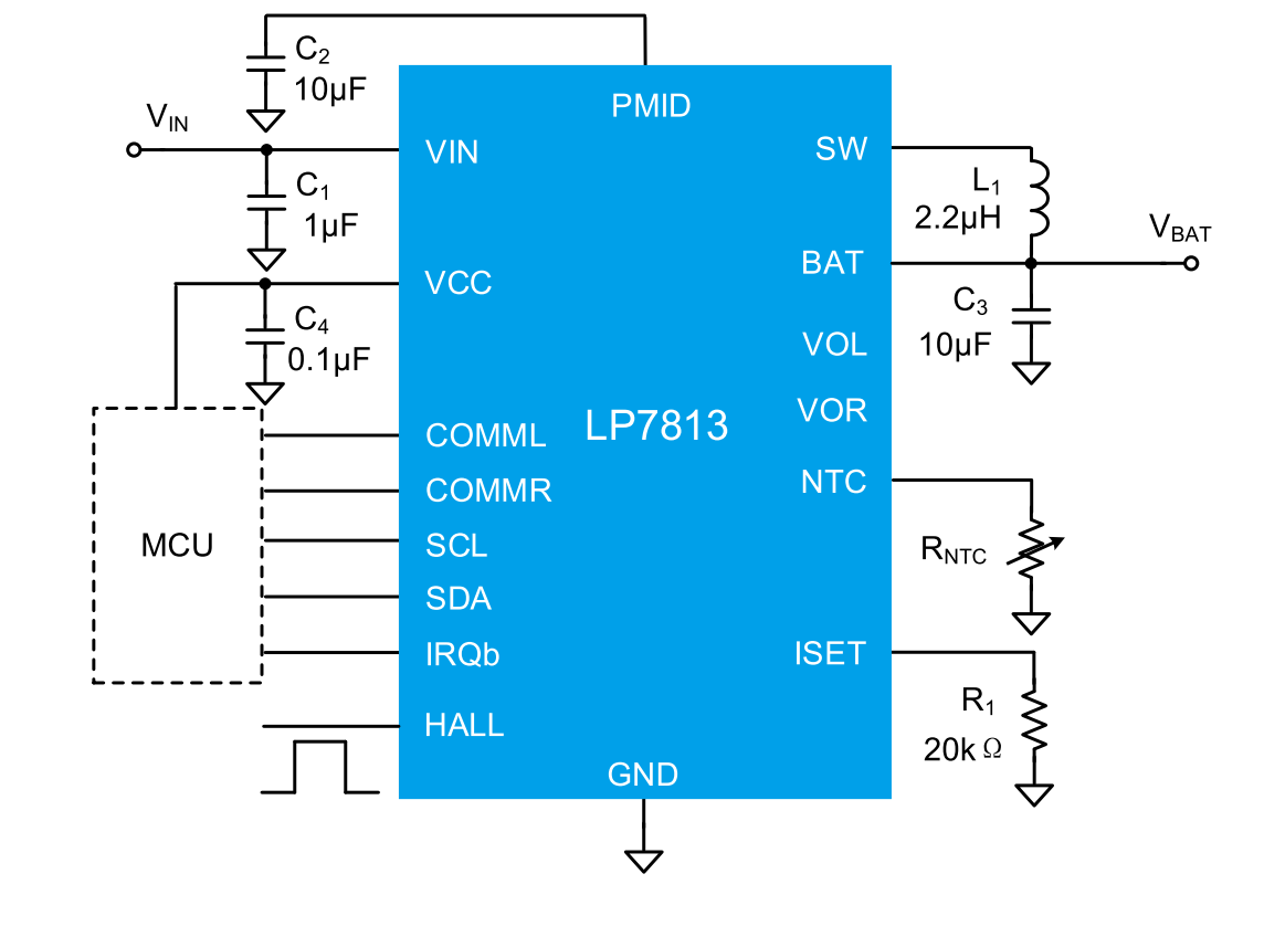
The LP7813 is a fully integrated switch mode charger solution with power path management targeting TWS charging case applications. A low on-resistance BUS-FET is integrated to manage the input power from the VIN pin. A bidirectional buck or boost converter is integrated to manage charging and discharging of the battery. The buck charger supports up to 1A charging current with up to 95% efficiency. The ultra-low quiescent current boost converter consumes less than 2μA quiescent current and supports up to 0.6A output current. Two independent load switches feature earphone insert detection, removal detection and provide power from the PMID pin to the VOL pin and VOR pin with ultra-low voltage drop. An NTC circuit is offered to manage the temperature range that charging or discharging is allowed. A VCC pin delivers power to the system that contains an MCU typically. The LP7813 offers power path management that allows the system to be powered up with a fully-discharged battery. It can dynamically manage the power from the VIN input and the battery to meet the system loading needs. An I2C interface enables programming various parameters of charging, discharging, and multiple protection functions. An interrupt output (IRQb) sends a signal to the MCU when an interrupt event happens so the MCU can take actions accordingly. The LP7813 support ship mode by setting the SHIP bit and support three methods to exit ship mode.
Multiple features are offered for the safe operation of the system, including input voltage OVP (over voltage protection), UVLO (under voltage lockout), OTP (over temperature protection), SCP (short circuit protection), etc. When powered by a battery, LP7813 can operate with only 5-µA current and this current is reduced to 0.7-µA when in ship mode.
The whole System is in a 16-pin 3 X 3 QFN package.